Page 2 of 2
Re: Schematics of Espressif ESP32 dev boards & modules
Posted: Wed Jul 12, 2017 2:32 pm
by rudi ;-)
Hi Angus
i wounder me - does we have Shematic V3 Wrover-Kit
do you know ( cause
SW1 problem ) i would look up -
txs
best wishes
rudi

Re: Schematics of Espressif ESP32 dev boards & modules
Posted: Wed Jul 12, 2017 2:57 pm
by loboris
https://dl.espressif.com/dl/schematics/ ... _SCH-3.pdf
I have no problem with SW1, except when sdcard is in socket and initialized.
Re: Schematics of Espressif ESP32 dev boards & modules
Posted: Thu Jul 13, 2017 9:37 am
by Angus
Thanks loboris, I'd forgotten to add a link to the first post (added now).
Re: Schematics of Espressif ESP32 dev boards & modules
Posted: Sat Nov 24, 2018 5:52 pm
by _Prasad
Hi Angus,
Can you share the specs for the PCB antenna design? I don't have Pads software to read reference PCB design to measure the dimensions.
Thanks,
Prasad.
Re: Schematics of Espressif ESP32 dev boards & modules
Posted: Mon Nov 26, 2018 4:33 am
by Angus
Hi Prasad,
Can you share the specs for the PCB antenna design? I don't have Pads software to read reference PCB design to measure the dimensions.
The Reference Designs should include a directory with design files in the industry standard Gerber format. A Gerber viewer (free ones available for most platforms) should allow you to look at the specific dimensions of the PCB antenna.
Note that PCB antenna design can be PCB fabrication process dependent, so you may need to test prototypes and tweak them a little to get optimal performance.
Re: Schematics of Espressif ESP32 dev boards & modules
Posted: Mon Nov 26, 2018 4:34 am
by Angus
Note that this post hasn't been updated lately as Reference Designs are now available on the Espressif web site:
http://espressif.com/en/support/download/documents
Re: Schematics of Espressif ESP32 dev boards & modules
Posted: Tue Nov 27, 2018 3:45 pm
by _Prasad
Ohh why didn't i notice that. Dumb me

Thanks Angus, Just checked with KiCad Gerber Viewer and i can measure the antenna dimensions. Btw i have already sent one prototype to fab with TI's SWRA 117 reference antenna specs, lets see how that goes too

Re: Schematics of Espressif ESP32 dev boards & modules
Posted: Wed Nov 28, 2018 9:13 am
by _Prasad
Hi Angus,
Just for the reference here is my KiCad 3D rendering which i have already sent for fab. Indeed dimensions of this antenna is bit different from the reference antenna. but i'll post the result anyway when it arrived.
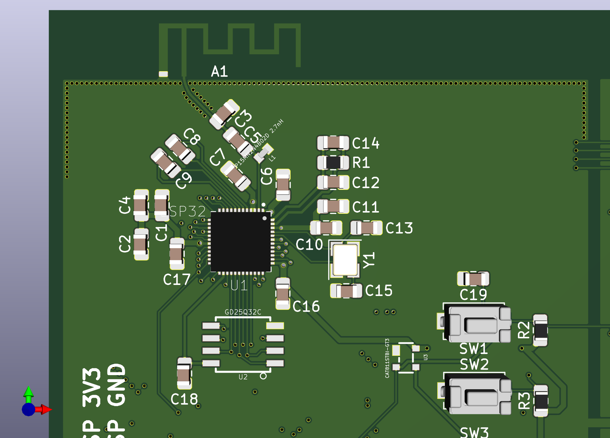
- 2.png (332.69 KiB) Viewed 13877 times
Thanks,
P .
Re: Schematics of Espressif ESP32 dev boards & modules
Posted: Sat Dec 22, 2018 2:52 pm
by _Prasad
Hi Angus,
I have assembled my PCB design with SWRA 117 antenna. And i must say it works a treat. I have tested bluetooth connection upto 20 meters with obstacles(Haven't tested with line of sight distance yet) and it maintained the connection.
Btw how do you define the optimal performance?
For the reference i used SWRA 117 antenna which came with KiCad default footprint library. And for the fab i used JLCPCB.
Having all that said i'm gonna change the antenna to the recommended dimensions when i'm doing the final miniaturized PCB design. This is more of a proof of concept of our product(rest of the PCB is a secret squirrel
).
Here is the picture of it,
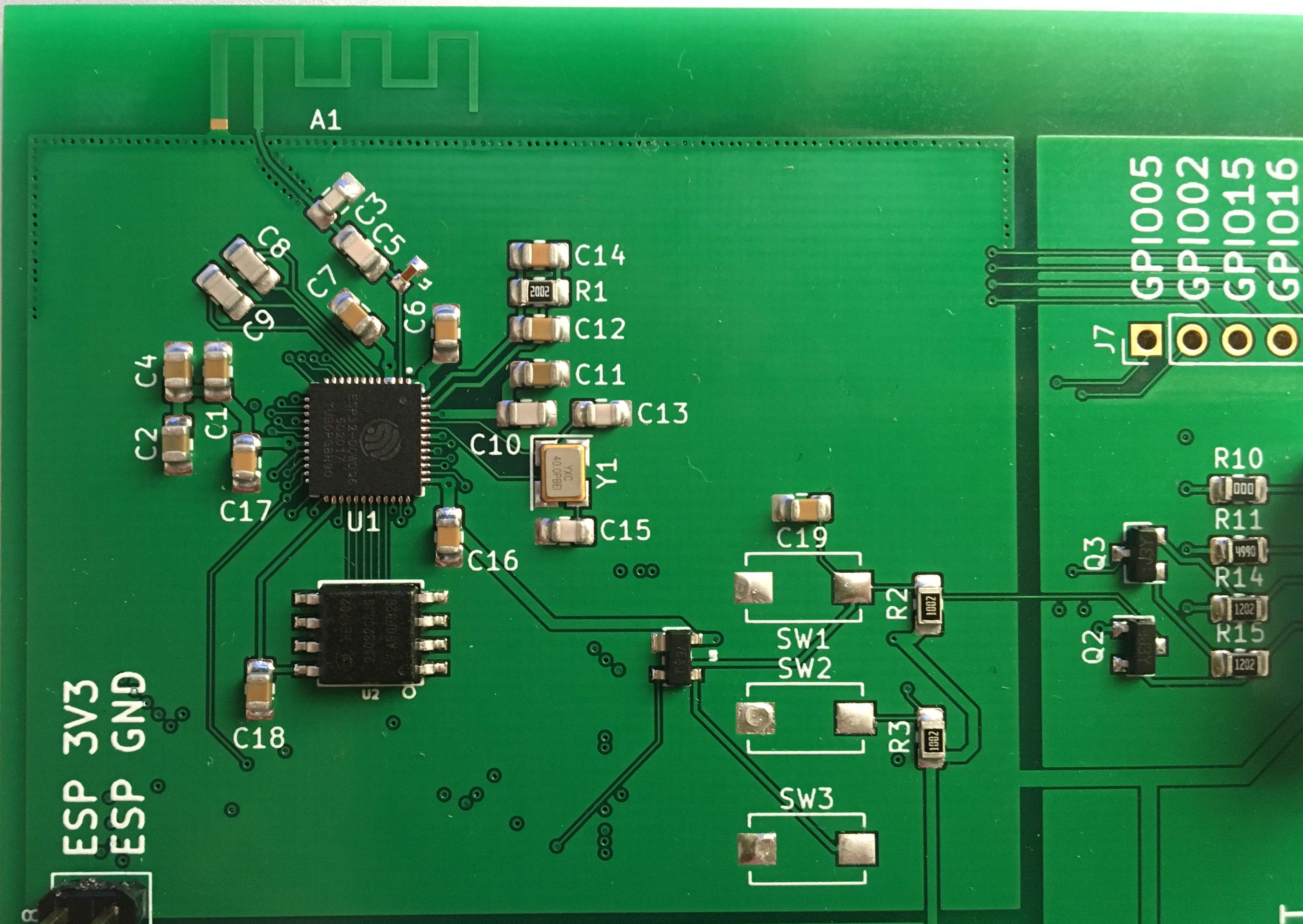
- 1.png (10.27 MiB) Viewed 13652 times
Kind Regards,
P.